
Equipment
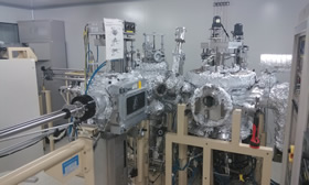
DC/RF magnetron sputtering system MPS-4000-HC7MPS-4000-HC7, produced by ULVAC Technologies in Japan, is a sputtering system with three chambers and seven targets inside that is suitable for ultrahigh vacuum as well as lower speed film deposition. Vacuum system comprise mechanical pumps, turbo molecular pumps and titanium sublimation pump. So base vacuum could attain 1E-6 Pa. Three chambers are preparation chamber, intermediate chamber and deposition chamber, respectively. Preparation chamber enables the capability of sample transfer in addition to sample clean via plasma. Inside intermediate chamber there is a four-inch target that could be used to deposit metal oxide thin film such as AlO and MgO. Deposition chamber consists of seven targets, providing the chances to deposit magnetic metal film and specific functional material film, for example NiFe, CoFeB, Pt, Ta. Threrfore this sputtering system could be used for researches of nano magnetic multilayers based on AMR, GMR and TMR
magnetron sputtering system by Kurt·J·Lesker
This magnetron sputtering system was designed by Kurt·J·Lesker, USA, manufactured and donated by SAE, Hong Kong. It includes control system and sputtering system. The control system is a PC program which could totally achieve remote control of the voltage, power, gas flux, pressure, sputtering time, etc. The sputtering system includes preparation chamber and sputtering chamber which are adapted to pre-vacuum-pumping and thin film growth respectively. There are 4 targets in the sputtering system including 2 DC and 2 RF targets which can implement the functions of metal materials and insulators growth respectively.
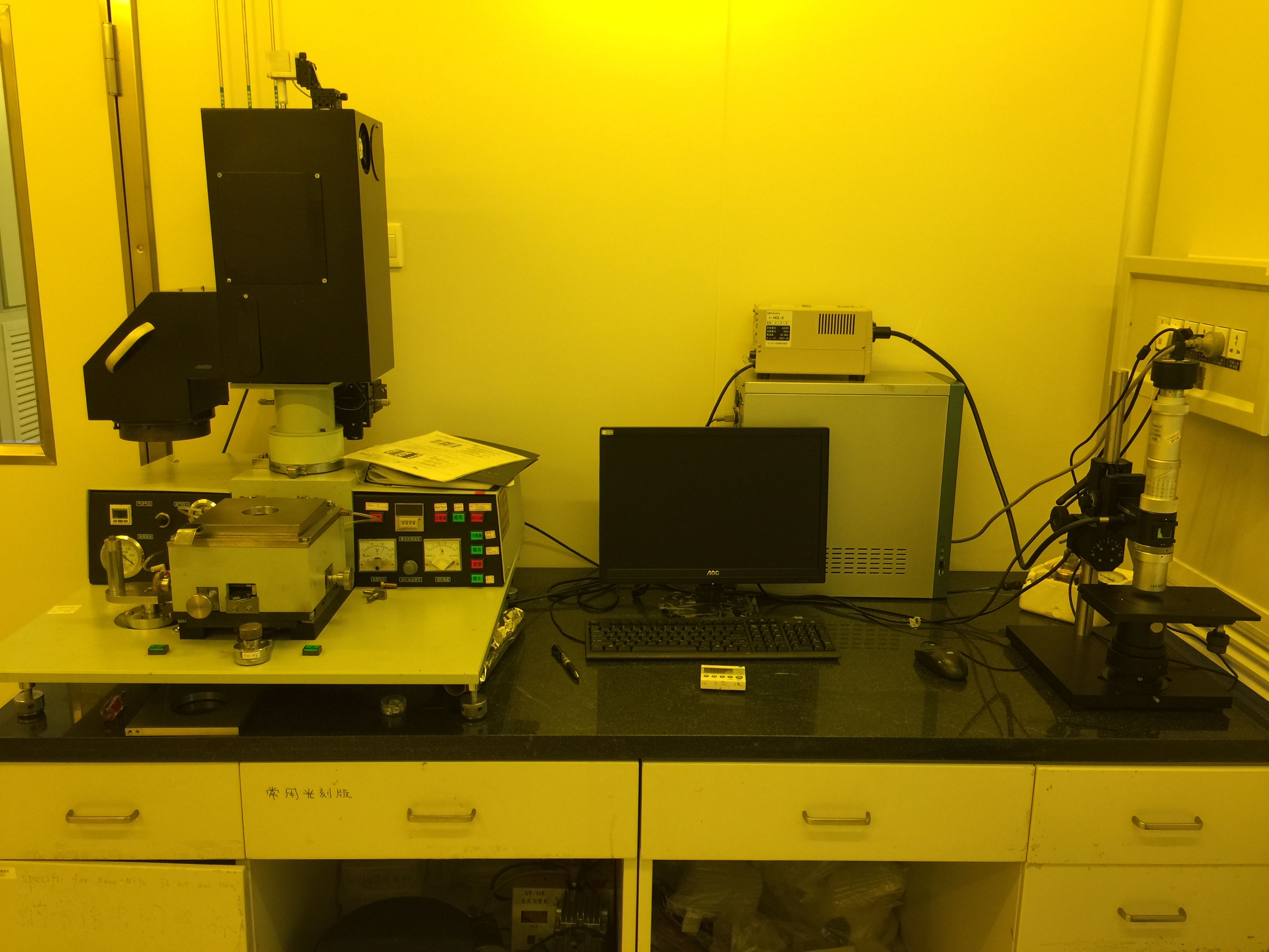
Domestic Deep-uv Exposure System:
The uv exposure system produced by chengdu xinnanguang optical company, comprising displacement platform of three degrees of freedom, the ultraviolet emission system, high-precision CCD imaging system, could achieve contact exposure in a more accurate means, of the precision level of 1 micron, and also can be used to make micron level of magnetic tunnel junction, Hall bar and other pattern of micron scale device. The use of resist in the system, such as the positive resist S1813, negative resist N440, AZ512, etc., can realize the exposure of different precision and line width.
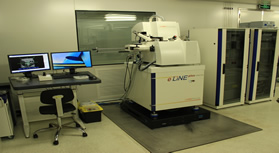
Nano-patterning and Ultra-wideband Electromagnetic Measurement System (Public measurement platform, maintained in super-clean room of M02 group)
The e-LiNE plus CAS system is developed with the support of “The Major Scientific Equipment and Instrument Development Project”. It is able to fabricate 10-nm-wide lines with electron exposure and perform the AC and DC electrical transportation measurement under ±300 Oe magnetic field or electrical field. The stitching and overlay of the electron beam lithography could reach the order of 10 nm. The frequency adopted vary from 0 to 40 GHz. The basic electron beam system could load 30 kV high voltage and detect the electrons with a secondary electron detector. The CAS owns the independent intellectual property rights of this system.
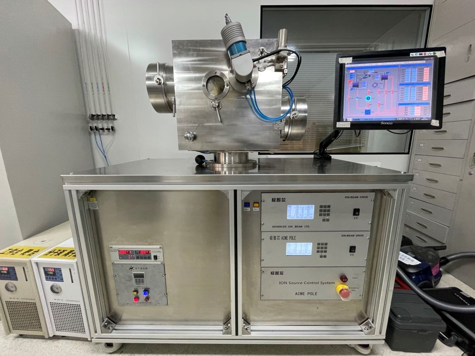
Ar-ion etching machine
This machine is developed and produced by Advanced Inc. In order to etch the sample, the Ar-ion plasma is first created from the Ar source through voltage excitation and then bombard the surface of the sample with high speed accelerated by the electric field. This machine is equipped with independent cooling system, so it’s able to conduct continuously etching. Working capability, Ion energy: 100-650 eV, Ar-ion beam density: 0.2-0.7 mA/cm2, etching uniformity: ±5% (For 4-inch wafer), Maximum vacuum: 8.5*10^-5 Pa (45 mins from atm to 5*10^-4 Pa ), holder cooling temperature: 5 - 25 ℃, holder rotation speed: 9 rpm, holder inclination angle 0 – 90°, to meet various micro-fabrication requirements for different thin film.
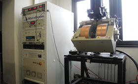
Vibrating sample magnetometer (MicroSense EZ-VSM)
Vibrating sample magnetometer (MicroSense EZ-VSM) can measure basic magnetic parameters: for example, hysteresis loops and small hysteresis loop, IRM and DCD remanence curves, SFD, Delta M, Delta H, Henkel Plots, variable angle and AC remanence curves, temperature scans and other tests. Maximum magnetic field: 2.2T, sensitivity: 1E-6 emu, temperature range: 350-770K, automatic angle: 360 degrees. By using the electromagnetic induction principle, the magnetic moment of the sample can be detected by induced voltage signals in the coil, so that it can measure the magnetic moment of the sample at a fixed frequency and amplitude,.
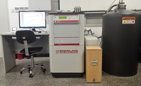
PPMS
Physical Property Measurement System (PPMS) is designed and manufactured by Quantum Design. It is a platform providing low temperature and strong magnetic field, integrated automatic magnetic, electrical, thermal and morphological, and even ferroelectric and dielectric and other physical measurement means. Main parameters include: Magnetic field: ±9 T; Temperature: 1.9 K—400 K; Fundamental measurement: DC resistivity, R(T), R(H), R(θ); Expand options: rotational sample holder, VSM.
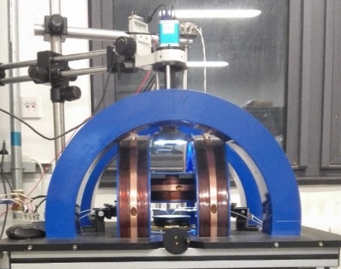
3D magnetic field probe platform
The platform consists of three orthogonal Helmholtz coils that produce magnetic fields of X, Y and Z, respectively. The magnetic field of the Helmholtz coil is no hysteresis and the magnetic field has good linear response with the current, which is very suitable for the measurement of linear magnetic field sensors. The maximum magnetic field can reach 350 Oe in the three direction and the field resolution is about 0.05 Oe
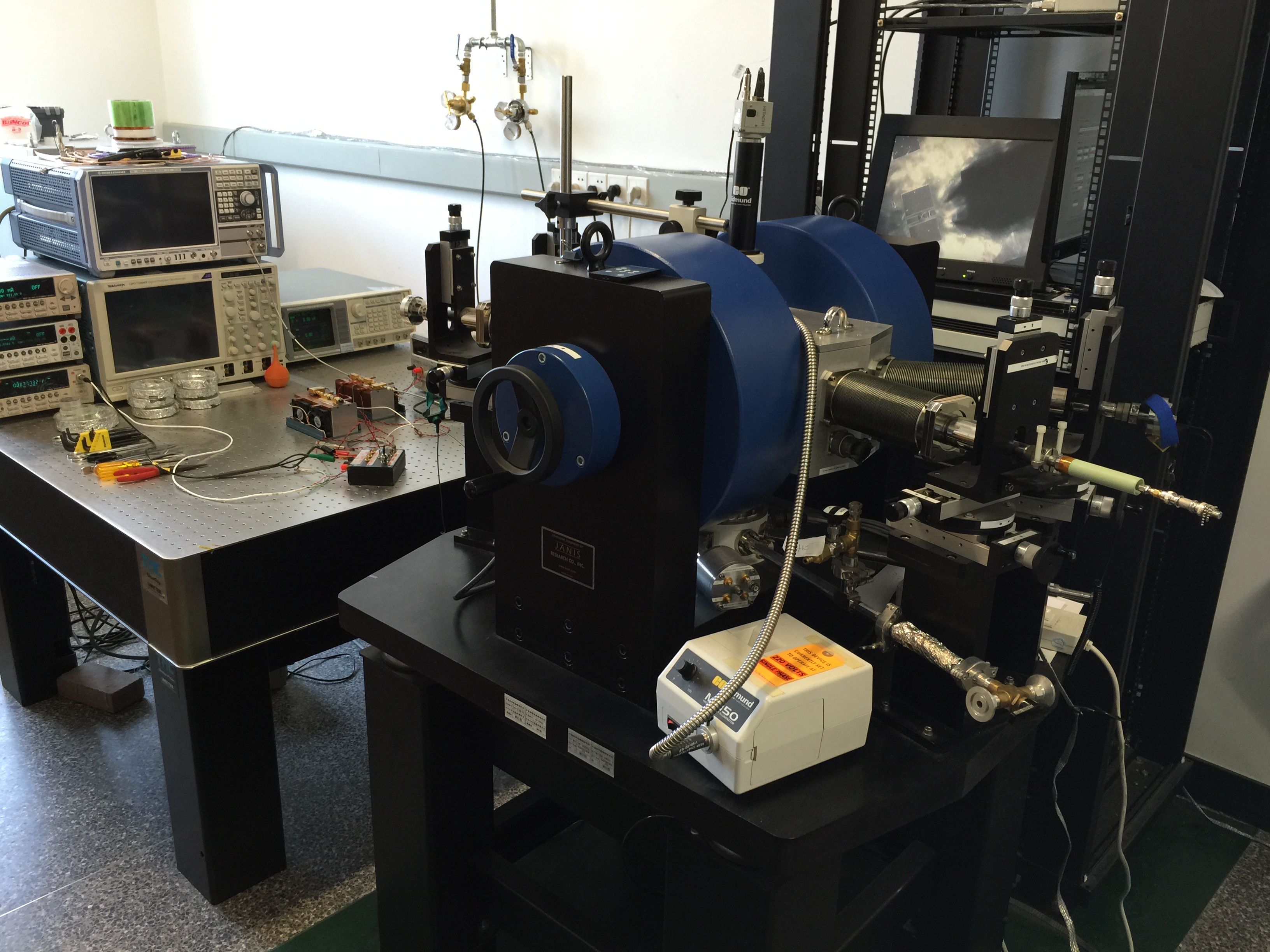
High Frequency Measurement Platform:
High Frequency Measurement Platform was designed and developed by M02 Group, IOP, and Janis, USA. This measurement system includes 4-probes measurement platform, temperature control module, magnetic field control module, DC measurement module and microwave measurement module. Its probes are capable of non-destructive transmission of the GHz-order high-frequency signal. Cooperating with high frequency instruments such as vector network analyzer, signal/spectrum analyzer, and lock-in amplifier, it can realize the functions of ferromagnetic resonance, spin rectification and spin nano oscillators measurements.
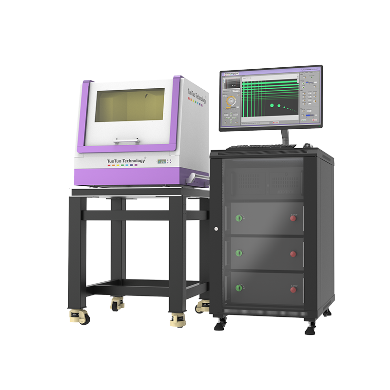
Maskless lithography machine TTT-07-UV Litho-ACA
The model TTT-07-UV Litho-ACA maskless lithography machine manufactured by Toto Technology has the advantages of high flexibility, high precision and maskless, which is very suitable for scientific research. The lithography feature size is 1μm, the lithography area can reach 6 inches, high precision step lithography, no mask lithography.
地址:北京市海淀区中关村南三街8号 中国科学院物理研究所M02组 邮编100190 电话:+86-10-82649268 传真:+86-10-82649485 电子邮件:xfhan@iphy.ac.cn